| Model: | ONE-10 |
|---|---|
| Brand: | ONESEINE |
| Origin: | Made In China |
| Category: | Electronics & Electricity / Electronic Components / Circuit Board |
| Label: | Multilayer PCB , 8 layer PCB , Multilayer Printed |
| Price: |
US $11
/ pc
|
| Min. Order: | 1 pc |
| Last Online:03 Sep, 2018 |
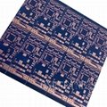
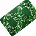
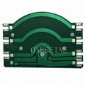
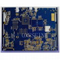
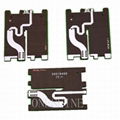
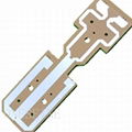
8 Layer Gold Plated PCB Multilayer Printed Circuit Boards Fabrication
PCB information:
Material: FR4 3 core ,6 layers,fake 8 layers
Surface finish:Gold plated
Copper weight:2OZ
Color: Black and white silkscreen
Board size:6*6cm
Stack up layer information as follow:
NO.1
1 Signal 1 component side, microstrip trace layer
2 Signal 2 internal microstrip trace layer, better trace layer (X direction)
3 Ground
4 Signal 3 stripline routing layer, better trace layer (Y direction)
5 Signal 4 Stripline Layer
6 Power
7 Signal 5 Internal Microstrip Trace Layer
8 Signal 6 Microstrip Trace Layer
NO.2
1 Signal 1 component SIDE, microstrip trace layer, good trace layer
2 Ground layer, better electromagnetic wave absorption capacity
3 Signal 2 stripline routing layer, good routing layer
4 Power power layer, and the underlying stratum constitute excellent electromagnetic absorption
5 Ground layer
6 Signal 3 stripline routing layer, good routing layer
7 Power Formations with Large Power Supply Impedance
NO.3
This is not a good way to stack boards due to poor electromagnetic absorption capability and large power supply impedance. Structure as follows:
1 Signal 1 component side, microstrip trace layer
2 Signal 2 internal microstrip trace layer, better trace layer (X direction)
3 Ground
4 Signal 3 stripline routing layer, better trace layer (Y direction)
5 Signal 4 Stripline Layer
6 Power
7 Signal 5 Internal Microstrip Trace Layer
8 Signal 6 Microstrip Trace Layer
NO.4
It is a variant of the third stacking mode. Since the reference layer is added and the EMI performance is better, the characteristic impedance of each signal layer can be well controlled.
1 Signal 1 component side, microstrip trace layer, good trace layer
2 Ground formation, better electromagnetic wave absorption capacity
3 Signal 2 stripline routing layer, good routing layer
4 Power power layer, and the underlying stratum constitute excellent electromagnetic absorption
5 Ground
6 Signal 3 stripline routing layer, good routing layer
7 Power layer with Large Power Supply Impedance
www.oneseine.com
