| Model: | - |
|---|---|
| Brand: | JHYPCB |
| Origin: | Made In China |
| Category: | Electronics & Electricity / Electronic Components / Circuit Board |
| Label: | HDI PCB , HDI Circuit Board , PCB Manufacturer |
| Price: |
-
|
| Min. Order: | 1 pc |
| Last Online:26 Jul, 2024 |
JingHongYi PCB (HK) Co., Limited
Electronic PCB Board, HDI PCB, HDI Printed Circuit Board, HDI Circuit Board
we are specialized manufacturers from China, Electronic PCB Board, HDI PCB suppliers/factory, wholesale high-quality products of HDI Printed Circuit Board R & D and manufacturing, we have the perfect after-sales service and technical support. Look forward to your cooperation!
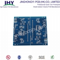
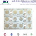
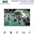
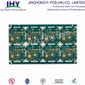
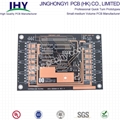
HDI PCB 6 Layer Immersion Gold
HDI stands for High Density Interconnector, HDI Printed Circuit Board. A circuit board which has a higher wiring density per unit area as opposed to conventional board is called as HDI PCB. HDI PCBs have finer spaces and lines, minor vias and capture pads and higher connection pad density. It is helpful in enhancing electrical performance and reduction in weight and size of the equipment. HDI PCB is the better option for high-layer count and costly laminated boards.
High density interconnect (HDI) PCBs represent one of the fastest-growing segments of the Printed Circuit Board market. Because of its higher circuitry density, the HDI PCB design can incorporate finer lines and spaces, smaller vias and capture pads, and higher connection pad densities. A high-density PCB features blind and buried vias and often contains microvias that are .006 in diameter or even less.
Regarding the electrical needs of high-speed signal, the board should have various features i.e. high-frequency transmission capability, impedance control, decreases redundant radiation, etc. The board should be enhanced in the density because of the miniaturization and arrays of the electronic parts. In addition, to the result of the assembling techniques of leadless, fine pitch package and direct chip bonding, the board is even featured with exceptional high-density.
There were a lot of different names for the PCB with such structures. For example, it was called SBU (Sequence Build up the Process) in European and American industry as the program production is in the constructive mode of sequence. It was called MVP (Microvia Process) in Japanese industry because the hole of such products is much smaller than the previous one. It was also called BUM (Build up Multilayer PCB Board ) because the traditional multilayer is known as MLB (Multilayer PCB Board).In order to avoid confusion, IPC Printed Circuit Association proposed to call it HDI (High Density Interconnection Technology) as the common name, but it can not reflect the characteristics of the circuit board. So the majority in the PCB industry define such products as HDI PCB.
Innumerable benefits are associated with HDI PCB, like high speed, small size and high frequency. It is the primary part of portable computers, personal computers, and mobile phones. Currently, HDI PCB is extensively used in other end user products i.e. as MP3 players and game consoles, etc.
| Payment Terms: | TT/LC/DP/DA |
|---|---|
