Product Center
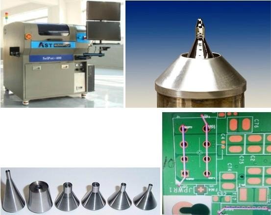
AST selective wave soldering
Selective wave soldering:
Selective wave soldering refers to the welding of the device on the surface of the patch on the surface. Selective wave soldering machine through the solder joint selective partial spray flux and solder, if necessary, can also the preheating of circuit board.
The benefit of such a solder is: first, no special template or tool is required. Secondly, the process parameters of each solder joint can be set according to the requirements of the welding components, so that the quality of the whole board can be improved greatly.
Most of the through-hole soldering technology selective, soldering form by As 3 process:
As with most of the through hole welding process, selection is divided into 3 parts, spray flux, preheating welding, soldering
Preheating, and soldering Fluxing
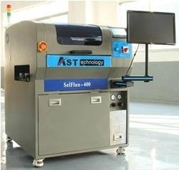
Fluxing - flux spray coating
Jet flux injection nozzle, moving under the PCB as programmed path, spray flux to selected area under PCB. Moving path can be set, X / y mobile platform, according to the program of the flux coated
Fluxing spray
Moving path, speed and flux flow, air pressure are settable. spray path and movement speed and flux flow and air pressure can be set. The same piece of PCB board, according to the needs of different amount of welding flux.
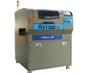
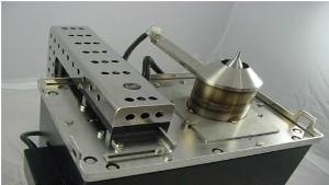
Preheating preheating
Ways for preheating as wave solder IR, or hot air convection. Two
Two ways of preheating, infrared or hot air.
PCB heat capacity set, different preheat temperature and time for PCB. According
According to the heat absorption of PCB plate, the heating temperature and the heating time of the components are set up.
1 improve the process activity of ji,
2 increase the wetting properties of pad
Soldering welding
Pot under the work of X/Y/X moving table melting, soldering come from standard or customized nozzle moving, under the PCB as programmed path soldering, to required components at PCB. Solder
Mobile path can be set, X/Y/Z platform for mobile, for the point of the programming welding.
Path moving, speed soldering, temperaure wave, temperature N2, height are settable. moving
Moving path, moving speed, solder temperature, nitrogen temperature, peak height can be set. The same PCB board can set different welding speed to get the different requirements of the solder joint. For example, the large heat absorbing pads, welding speed can be set more slowly, small welding plate welding can go faster.
Advantages and disadvantages of selective wave soldering:
Advantage advantages:
The welding parameters of each solder joint can be customized, we don't have to do with it ". Engineers have enough technology to adjust the space of each solder joint welding parameters (flux of spray volume, welding time, welding peak height) transferred to the best defect rate thereby reducing, we may even do through hole components of zero defect, welding
Selective soldering just according to the welding point of selective soldering flux spraying, circuit board cleanliness so greatly improved, also ion contamination greatly reduced. Flux Na is Na + and Cl negative chloride ions if the residue on the circuit board, a long time will combine with the water molecules in the air to form salt and corrosion circuit board and solder joints, resulting in open solder joints. For the backend does not cleaning products, choice of welding greatly reduces the flux residue.
The peak temperature of lead-free wave soldering is about 260. During welding, the temperature of the whole circuit board experienced from room temperature to 260 DEG C, and then cooled to room temperature, the rise and drop two temperature change process caused by thermal shock will make different material objects on the circuit board because of different thermal expansion coefficients and the formation of shear stress. When the shear stress to a certain extent will enable BGA stratification and the formation of micro cracks. Such defects are difficult to detect (even with the help of X and AOI), and the solder joints are still on the physical connection (it can not be detected by functional testing), but when the product is used in the solder joints are affected by external factors such as shock, it is easy to form an open circuit.
Selection of welding is only for specific points of the welding, whether in spot welding and welding are not on the whole piece of line heat shock, so it is not in the BGA and other surface mount devices to form a clear shear stress, thereby avoiding the thermal shock caused by various defects.
Summary
In the end whether the use of selective soldering technology? To make this decision, you may need to consider the following:
1 high quality requirements for welding through hole components.
2 for the conventional welding method is not ideal for the treatment of thick plate, large heat absorbing plate, large heat absorbing parts, high component plate, characteristic difference of larger components.
The 3 existing PCB board type is various, into a larger fixture.
4 on the surface of the patch line on the number of holes in the device or the number of solder joints, PCB board to complete the TIME CYCLE can meet the requirements of production capacity.
5 if there is no cleaning process, the surface of the PCB plate welding after the completion of the surface cleanliness.
6.PCB board components have not sticky flux such as open potentiometer, adjustable resistor, the components can not be heated.
