| Model: | - |
|---|---|
| Brand: | - |
| Origin: | Made In China |
| Category: | Electronics & Electricity / Electronic Components / Circuit Board |
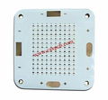
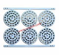
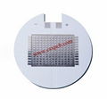
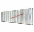
| Label: | FR4 PCB |
| Price: |
-
|
| Min. Order: | - |
Product Description
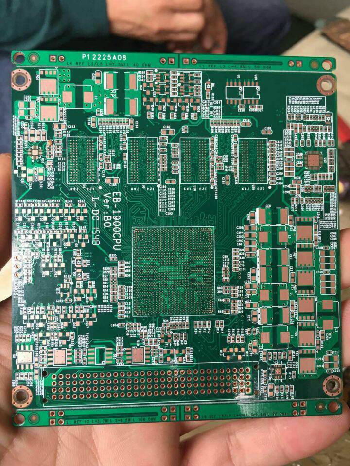
1.Drawing format: Protel 98 or 99 or 99 SE/Protel DXP or DXP 2004/Allegro/Power PCB/CAM 350/Gerber(favorite) ;
2.Layer: single/double/four/six/eight/ten/twelve/fourteen/sixteen/eighteen/twenty…… ;
3.Copper thickness(I/O): 18um/0.5oz、35um/1oz、70um/2oz、105um/3oz、140um/4oz、175um/5oz、210um/6oz;
4.Laminate type: FR4 /IT180A/ FR4(halogen-free)/FR4 (halogen-free)+high-Tg/Rogers/Arlon/Tyconic/Nelco…… ;
5.Board thickness: 0.2mm/0.5mm/0.7mm/0.8mm/1.0mm/1.2mm/1.5mm/1.6mm/2.0mm/2.4mm/3.2mm/6.4mm ;
Note: (1) If no special requirement for structure or no impedance requirements, the board thickness will be finished with1.6mm commonly; and if more than 14 layers, the board thickness should not be less than 1.6mm.
(2)If without notes, the tolerance of board thickness will be not more than ±10%.
6.Surface finish: HASL/HASL(lead-free)/Immersion Sn/Immersion Au/Immersion Ag/Au plated/OSP…… ;
7. Solder mask: solder resist ink/blue gel/carbon ink print; Color: Green(light/matte)、Black、White、Yellow、Blue、Red ;
8. Silkscreen legend: White/Yellow/Black;
Note: If green soldermask, the legend will be printed in white; if white soldermask, the legend will be black.
9.Min diameter of Via hole: mechanical hole-6mil/laser drilling-4mil; maximal capability:1:10(thickness-diameter ratio);
10. Soldermask for via hole: (1) PCB design request,(2) Cover holes by soldermask,(3) Clogging, (4) plug for via hole of BGA;
11.NPTH: If any NPTH, pls mark the NPTH;
12. LOGO and lead time: If no customers demand, manufacter's LOGO and time will be as the default.
13. Chamfer of goldfinger: Corner cut processing: 20°、30°、45°……, please note the depth and the angular;
14. Panel drawing: pcs/set; If the dimension of each pcs between 50mm×50mm and 125mm×150mm, we advice to adopt delivery in unit of "set(A*B)"; and if more than 200mm×165mm, deliery in unit of "pcs" will be popular;
15. plate edge procesing: there are two cases that we advice to add 5mm width edge in each length direction: (1) if the printed board will be undergone the reflow soldering, and the distance between components and plate adge is less than 5mm;
(2) if the printed board will be undergone the wave-soldering, and the distance between components and plate edge is less than 3mm.
16. Acceptance Criteria: (1) Based on the customers demand; (2) IPC-A-600G; if no special requirement, the Ⅱ grade standard
will be the default criteria.
17. Test: E-test、Impedance test、Hi-pot、Solderability test、Thermal stress test、Insulation resistance test;
For any matters not mentioned herein, please feel free to contact us!
| Payment Terms: | T/T |
|---|---|
Member Information
| Shenzhen Chuangsanxin Technology Co., Ltd. | |
|---|---|
| Country/Region: | Guang Dong - China |
| Business Nature: | Manufacturer |
| Phone: | 15875508614 |
| Contact: | Song (Sales) |
| Last Online: | 09 Jul, 2016 |


