| Model: | - |
|---|---|
| Brand: | - |
| Origin: | - |
| Category: | Electronics & Electricity / Electronic Components / Circuit Board |
| Label: | PCB |
| Price: |
¥100
/ pc
|
| Min. Order: | 1 pc |
Product Description
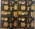
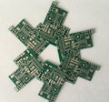
High Density Interconnect PCB
General Information for High density pcb (HDI PCB)
HDI pcb is the abbreviation for High Density Interconnect pcb or High Density pcb.An HDI PCB is defined as a printed circuit board with a higher wiring density per unit area than a conventional PCB.
HDI includes the use of fine features or signal traces and spaces of 0.003” (75 µm) or less and laser-drilled blind or buried microvia technology. Microvias allow the use of micro-interconnects from one layer to another within a PCB utilizing a smaller pad diameter creating additional routing density or reducing form factor.
High Density PCB is used extensively in applications and industries including:
| ● Cell phone | ● GPS |
| ● Telecom | ● ASemiconductor |
| ● Automotive | ● Military |
| ● Medical | ● Instrumentation |
1. 6L HDI printed circuit board for Intercom

6L High density PCB (HDI PCB) for intercom
Board dimensions: 110 x 166mm
Finished board thickness: 1.2mm
Material: FR-4 Tg150
Minimum holes size: 0.1mm
Minimum line width/clearance: 3.5/3.5mil
Copper thickness: 1oz
Solder mask: top and bottom (color: green)
Silkscreen: top (color: white)
Finish: immersion gold (top and bottom)
Board stack up: 1 + 4 + 1
2. 6 Layers HDI PCB
 6L High density PCB (HDI PCB) for intercom
Board dimensions: 80 x 120mm
Finished board thickness: 1.0mm
Material: FR-4 Tg150 halogen free
Minimum holes size: 0.1mm
Minimum line width/clearance: 2/3mil
Copper thickness: T oz (12um)
Solder mask: top and bottom (color: Blue)
Silkscreen: top (color: white)
Finish: immersion gold (top and bottom)
Board stack up: 1 + 4 + 1
3. 8L Cell phone HDI board PCB

8layers High density PCB (HDI PCB) for cell phone
Base material: FR4, Tg150
Layer count: 8 layers (HDI PCB)
Surface finishing: immersion gold
Board thickness: 1.0mm
Copper thickness: 0.5oz
Minimum line width: 0.075mm
Minimum line spacing: 0.075mm
Laser drilling + blind and buried drilling Impedance control
Stack up: 1+6+1
4. 10L High density printed circuit board

10layers HDI PCB
Base material: FR4, Tg170
Surface finishing: immersion gold
Board thickness: 1.0mm
Copper thickness: 0.5oz
Minimum line width: 0.1mm
Minimum line spacing: 0.1mm
Laser drilling + blind and buried drilling Impedance control
Board stack up: 1+8+1
Impedance control
5. 10L High Density Interconnect pcb

10L High Density Interconnect board
Laminate: FR4, Tg150
Board thickness: 1.6mm
Copper thickness: 17.5um (Hoz) for all layers
Solder resist: green color
Surface Finish: Immersion gold
Trace width/width: 0.89/0.1mm
Min. holes:0.1mm
Controlled Impedance
Board stack up: 1+1+6+1+1
Application: Industry control
6. 10L stage 2 Automotive HDI PCB

Layer count: 2 stage 10 layer
Board thickness:1.0mm
Dimension:160*130mm
Raw material:FR4 EM825
Copper thickness on the board surface:≥35um
Copper thickness in the hole barrel:20um
Min.line width/space:0.075mm
Minimum hole diameter:0.1mm
Surface finishing:immersion gold≥2u"
Application:automotive driving recorder
7. 10L every layer interconnection(ELIC) HDI PCB

Layer count: 10 layer
Board thickness:0.80mm
Raw material:FR4 370HR
Min.line width/space:0.075/0.075mm
Minimum hole diameter:0.10mm
Surface finishing:ENIG
Plug via-in-pad by resin and plate flat
Member Information
| Sandou Technology Co.,Ltd. | |
|---|---|
| Country/Region: | Guang Dong - China |
| Business Nature: | Manufacturer |
| Phone: | 18680210357 |
| Contact: | Ailen (Sales) |
| Last Online: | 04 May, 2018 |


