| Model: | - |
|---|---|
| Brand: | - |
| Origin: | Made In China |
| Category: | Electronics & Electricity / Electronic Components / Other Electronic Components |
| Label: | Sapphire wafer , GaAs wafer , InP wafer |
| Price: |
-
|
| Min. Order: | - |
Product Description
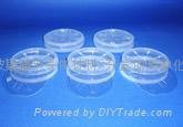
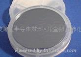
We are professional manufacturer of Epi-Ready Sapphire wafers,GaAs wafers, Ge wafers and InP wafers.Our headquarters is located in USA
We are producing:Epistone epi-ready wafer typical spec summary
a). C-plane 0.20 or 0.30 off to M
Surface Orientation C[0001] off M [1-100] 0.20 ± 0.10(target ± 0.050) / 0.30 ± 0.10
Diameter 50.8mm ± 0.1mm
Thickness 430um ± 10um
Major Flat A [11-20] ± 0.5°
Major Flat Length 16.0mm ± 1.0mm
Front Surface Finish Epi-ready polished, Ra< 0.2 nm
Back Surface SSP: Fine ground, Ra 0.4 to 1.0 um; DSP: Epi polished
Edge condition Edge defects not to exceed SEMI M3-91
Flatness TTV<10um, BOW <10um, Warp<10um
b). R-plane ±0.10
Surface Orientation R[1-102] ± 0.10
Diameter 50.8mm ± 0.1mm
Thickness 430um ± 10um
Major Flat 45°± 2° counter-clockwise from the projection of the C-axis onto the R-plane
Major Flat Length 16.0mm ± 1.0mm
Front Surface Finish Epi-ready polished, Ra< 0.3 nm
Back Surface SSP: Fine ground, Ra 0.4 to 1.0 um
Edge condition Edge defects not to exceed SEMI M3-91
Flatness TTV<10um, BOW <10um, Warp<10um
c). A-plane ±0.10
Surface Orientation A [11-20] ± 0.10
Diameter 50.8mm ± 0.1mm
Thickness 430um ± 10um
Major Flat C [0001] ± 0.5°
Major Flat Length 16.0mm ± 1.0mm
Front Surface Finish Epi-ready polished, Ra< 0.3 nm
Back Surface SSP: Fine ground, Ra 0.4 to 1.0 um
Edge condition Edge defects not to exceed SEMI M3-91
Flatness TTV<10um, BOW <10um, Warp<10um
C-plane, R-plane and A-plane Packaging
Packaged in a class 100 clean room environment, in single fluroware (samples) or cassettes of
25pcs (for official order) under a nitrogen atmosphere
1、2" , 3" , 4" Epi-ready Sahhpire wafers with 200/330/430/500um thickness.
2、2" , 3" , 4", 6" Epi-ready GaAs wafers with 325um to 675um thichness.
3、2" , 3" , 4" Epi-ready Ge wafers with 325/500um thickness.
4、2" , 3" , 4" Epi-ready InP wafers with 325/425um thickness.
5、All wafer specifications are adjustable to meet customers' special requirements.
6、Wafers Reclaim Service.
With our unique technology,the TTV、BOW and WARP of our wafers are all be controlled under 10um.The Ra of polished side can be controlled under 0.2nm.
Member Information
| Epistone Comp-Semi Materials Company Ltd. | |
|---|---|
| Country/Region: | Guang Dong - China |
| Business Nature: | Manufacturer |
| Phone: | 86-0755-89922158 |
| Contact: | Miss Huang (Sales) |
| Last Online: | 08 Jan, 2010 |
Related Products of this Company
-
No Image
purchase for "4' sapphire window


