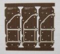
| Model: | 2-24 layer |
|---|---|
| Brand: | - |
| Origin: | Made In China |
| Category: | Electronics & Electricity / Electronic Components / Circuit Board |
| Label: | PCB , HDI , COB |
| Price: |
-
|
| Min. Order: | 100 pc |
Product Description
Technology and Capacities
Description
1 product range 2-24 Layers, HDI, Al Base, COB
2. Base Material FR-4 Glass Epoxy Laminate, Aluminum Based. (others by special order)
3. Major Laminate King Board(KB-6150/60) ShengYi(S1141,S1170) Rogers, High frequency Materials: PTFE, Getek, Nelco( by order)
4. Surface Finish Treatment Flash gold(Electrolytic) Electroless nickel immersion gold(Electroless ni/AU) OSP or Entek
Hot Air Leveling=(HAL-Tin/Lead)
Hot Air Leveling(Lead-free, Rohs)
Carbon Ink, Peelable MASK, Gold Finger. Immersion silver, Immersion Tin
5. Via Holes Copper PTH/Blind Via/ Buried Via/ HDI 2+n+2 with IVH
6. Impedance Control Tol. +/-10%(min (+/-7 Ohm)
7. Solder Mask Liquid Photo-Image(LPI)
8 Profilling CNC Routing, V-Cutting, Punching, Push Back Punching, Connector chamfering
9. Max Board size 610*711mm
10,Mini Board Thickness 0.2mm(2 layers)/0.4mm (4 layerS) 0.9mm(8Layer)/1.2mm(10 layer)1.2mm(10 layers)/1.3mm(12 layers)/1.5mm (14 layers)/1.7mm (16layers) / 1.8mm/2.0mm(18layers)/2.2mm(20layers)/2.4mm(22layersr)/2.6mm(24layers)
11. Copper Foil Thickness 18um/35um/70um-245um( Outer layer 0.5oz-7oz)
18um/35um/70um-210um ( Inner layer:0.5oz-6oz)
12 Min Via size and type Dia 0.15mm( finished)
13. Min line width and spacing 0.1mm/0.10mm(4min/4mil)
14 minimum via hole size and pad via: dia 0.2mm/pad: dia 0.4mm HDI<0.1mm via
15 Minimum Hole Tolerance +/-0.05mm(NPTH) +/-0.076(PTH)
17 Hole to hole edge gap 0.8mm
18. Minimum Tooling Hole Diameter 1.5mm
19. Minimum Legend line width 0.15mm
20 Dimensional Tolerance Pouching :+/-0.1mm PTH(+/- 0.076MM) By drilling, NPTH(+/-0.05mm) by drilling, NPTH(+/-0.1mm) by pouching, Remark:6.00mm hole tolerance by routing is +/-0.13mm
21. Other Dimensions Unless other specified Outline tolerance:+/-0.13mm for routing.+/-0.15mm for punching
22. Minimum Annular Ring The least circular strip plane inner layer/ outer layer—component holes:0.2mm via holes:0.15mm
23.minimum copper trace width the least noticeable width of the conductor in a circuit path on the printed wiring board width spacing :0.18um/0.5oz. 35um/1 oz. 70um/2 oz. Singe Sided:0.15mm, 0.15mm, 0.2mm
24. Minimum Spacing The least distance between adjacent edge of conductors(not-center-to center) on a single layer of a printed wiring board double sided: 0.10/0.13mm 0.13/0.13mm
0.2/0.2m multilayer:0.10/0.13mm 0.13/0.13mm 0.2/0.2mm
25 Minimum SMT Pitch o.4mm
26. Minimum Solder mask double sided 0.25mm. Multilayer:0.25mm
27. Minimum Solder mask Double sided: pad width 0.1mm multilayer:0.075mm
28. Copper to board Gap 0.2mm
29. Copper to Hole Gap 0.2mm
30.minimum void/thermal gaps 0.2mm*0.2mm or diameter=0.5mm
31. Acid Trap Closed 0.2mm
32. Capacity 600000 square feet( month)
Member Information
| Standard Printed Circuit Board Ltd | |
|---|---|
| Country/Region: | Hong Kong S.A.R |
| Business Nature: | Manufacturer |
| Phone: | 852-852-21140529 |
| Contact: | Sarela (Sales Executive) |
| Last Online: | 17 Feb, 2009 |


