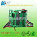
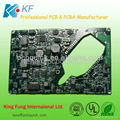
| Model: | KF-PCBA-004 |
|---|---|
| Brand: | KF |
| Origin: | Made In China |
| Category: | Electronics & Electricity / Electronic Components / Other Electronic Components |
| Label: | industrial drive pcb , pcb assembly factory , SMT/DIP PCBA |
| Price: |
-
|
| Min. Order: | 1 pc |
Product Description
Specifications:
1.Printed Circuit Board Fabricate/Assembly
2.safety&environmental
3.Competitive Price,High Quality
4.OEM Circuit Assembly
Product descriptions:
FR4 PCB SMT Assembly with high quality
Silk Screen:White
Solder Mask:Black
cooper:1oz 100% E-test
ENIG Surface Finishing
PCB SMT Assembly
Layers: 1-20 layer
Material:FR4,CEM-1,CEM-3,High TG150-170,Aluminum
Board thickness: 0.2-5mm
Copper: 0.5-3oz
Min holes:0.2mm for drill
Min line/space:4mil/4mil
Sloder mask:Green, Red, White, Yellow, Black, Blue,Mat Green...
Silkscreen: White, Yellow, Black, Red
Surface finish:HAL/HAL Leedfree,ENIG,Plating gold,Chem Tin/Ag,OSP
Outline Profile:CNC routing/V-Cut/Belveling/Punching
100% E-test: Flying probe test, Fixing test
Customed our products based on your need:material,specification,etc.
Welcome To K.F PCB Factory:
We are professional PCB manufacturer with ten years experiences .
Products range-single, double side ,multi-layer PCB ,flexible PCB and MCPCB.
We can provide fast prototype service – S/S in 24hrs , 4-8layers in 48-96 working
hrs production time .
1.PCB Made Ability:
|
Item |
Technical Standards |
||
|
Rise |
1-20 Layer |
||
|
Material |
FR-4,CEM-1,CEM-3,Hight TG,FR4 Halogen Free,FR-1,FR-2,Aluminum |
||
|
Thickness |
0.2mm-3.2mm(8mil-126mil) |
||
|
Minimum thickness |
0.075mm(3mil) |
||
|
Cu |
1/2 oz min;5 oz max |
||
|
Min line width/spacing |
0.075mm/0.1mm(3mil/4mil) |
||
|
Min drill hole |
0.2mm(8mil) |
||
|
Punching the smallest aperture |
0.9mm(35mil) |
||
|
Surface finish/treatment |
HALS/HALS lead free,Chemical tin,Chemical Gold,Immersion gold Inmersion Silver/Gold,Osp,Gold Plating |
||
|
The largest size puzzle |
610mm×508mm |
||
|
Tolerance |
Pore spaces |
+/-0.075mm(3mil) CNC Driling |
|
|
Line width |
+/-0.05mm(2mil) or |
||
|
+/-20% of original artwork |
|||
|
Aperture |
PTH L:+/-0.075mm(3mil) |
||
|
Non-PTH L:+/-0.05mm(2mil) |
|||
|
Appearance Tolerance |
+/-0.125mm(5mil) CNC Routing |
||
|
+/-0.15mm(6mil) by Punching |
|||
|
Warp |
0.70% |
||
|
Insulation Resistance |
10Kohm-20Mohm |
||
|
Conduction Resistance |
<50ohm |
||
|
Test voltage |
10-300V |
||
|
MLB |
Interlaminar deviation |
4 layers:0.15mm(6mil)max |
|
|
6 layers:0.25mm(10mil)max |
|||
2.Detailed Terms for Pcb Assembly
Technical Requirement:
1) Professional Surface-mounting and Through-hole soldering Technology
2) Various sizes like 1206,0805,0603 components SMT technology
3) ICT(In Circuit Test),FCT(Functional Circuit Test) technology.
4) PCB Assembly With UL,CE,FCC,Rohs Approval
5) Nitrogen gas reflow soldering technology for SMT.
6) High Standard SMT&Solder Assembly Line
7) High density interconnected board placement technology capacity.
Production Requirement:
1) Gerber file and Bom list
2) PNP Files,clear pics needed for pcba
3) Testing method for products
4.Packaging & Delivery:
| Packaging Details: | vacuum sealed packaging,silicagel inside |
|---|---|
| Delivery Detail: | Lead time according to order volum&board specifications |
Member Information
| Shenzhen King Fung Technology Co., Ltd | |
|---|---|
| Country/Region: | Guang Dong - China |
| Business Nature: | Trading Company |
| Phone: | 15220187273 |
| Contact: | lenaluo (sales) |
| Last Online: | 17 Sep, 2013 |


