| Model: | - |
|---|---|
| Brand: | - |
| Origin: | Made In China |
| Category: | Electronics & Electricity / Electronic Components / Circuit Board |
| Label: | metal base pcb , 4 layer flex pcb , double pcb |
| Price: |
-
|
| Min. Order: | - |
Product Description
Speedapcb - The best PCB manufacturers in China, established in 2014, is located in Changsha, Hunan Province. The company focuses on high-speed PCB design, printed circuit board manufacturing, SMT welding processing, and supply chain services. Products are widely used in communications equipment, computers and network equipment, consumer electronics, automotive electronics, industrial control, new energy, rail transportation, and other industries.
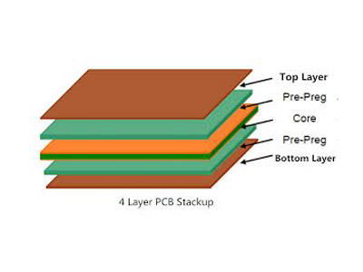
In general, in a 4 layer flex pcb, both the top and bottom layers belong to the signal layer, while another two inner layers are GND and VCC. If the first inner layer has several GND planes, the blank areas of which should be filled with copper. It could also have some routings, but do remember these routings are not allowed to cross the copper area. Same to the second layer with several powers. Usually, layers of a 4 layer PCB are connected by plated through holes, buried holes, and blind holes while layers of a 2 layer PCB are only connected by plated through holes. Besides, if possible, VCC and GND should not serve as signal layers.
There are insulation materials between the two layers. After every layer is printed with circuits, we could use lamination to make circuits overlap and use drills to make via holes to connect circuits. Since a 4 layer pcb layout, PCB has routings in several layers, it is a good choice if you want to design elaborate products in small sizes, like mobile phone circuit boards, mini-projectors, and recorders. In addition, multi-layers provide broader space for design, control differential characteristic and single-ended impedance, and better the output of signal frequency.
Right now, our electronic devices continue to pursue higher speed, larger capacity, and smaller size. Therefore, 4 layer pcb prototype is a product that emerges as the times require. Later plated through holes, buried holes and blind holes come into being to meet people’s needs to produce circuit boards with greater density, precision. Now that computer and aerospace industries are in great need of high-speed circuits, they are asking for components with higher packaging density. Besides, discrete components are getting smaller, microelectronics is facing rapid development, and electronic devices are turning into smaller and lighter ones. With such background, the single-sided or double-sided printed boards are not capable to increase the packaging density because they have restrictions brought up by limited space.
| Payment Terms: | T/T,Western Union, |
|---|---|
Member Information
| Hunan Speeda Technology Co.,Ltd. | |
|---|---|
| Country/Region: | Hu Nan - China |
| Business Nature: | Manufacturer |
| Phone: | 15387574935 |
| Contact: | Molly Tu (Sales Manager) |
| Last Online: | 19 Aug, 2020 |


