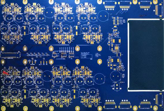
| Model: | - |
|---|---|
| Brand: | - |
| Origin: | Made In China |
| Category: | Electronics & Electricity / Electronic Components / Circuit Board |
| Label: | one layer pcb , pcb via plating , empty pcb board |
| Price: |
-
|
| Min. Order: | - |
Product Description
Speedapcb - The best PCB manufacturers in China, established in 2014, is located in Changsha, Hunan Province. The company focuses on high-speed PCB design, printed circuit board manufacturing, SMT welding processing, and supply chain services. Products are widely used in communications equipment, computers and network equipment, consumer electronics, automotive electronics, industrial control, new energy, rail transportation, and other industries. We also have rigid pcb fabrication, rigid circuit boards, rigid printed circuit board,etc.
PCB board can be divided into rigid pcb, motherboard pcb, flexible pcb (FPC) and rigid multilayer pcb according to the hardness.
Rigid pcb is often used as a motherboard. Generally, FR4 is used as the base material, and it cannot be bent. It is generally used in some places where relatively hard strength is required, such as computer motherboards and mobile phone motherboards.
SPEEDAPCB is a professional PCB supplier. We can provide customers with one-stop service from PCB design to PCB production and assembly.
HAVE A QUESTION OR REQUEST?
Click below, we’ll be happy to assist.
Features of Rigid PCB
As a professional PCB manufacturer, we have factories in Guangdong, Jiangxi, and Hunan, using advanced production equipment to ensure the high quality of our products. We have 10 PCB production lines, the machine works 24 hours a day, only to provide customers with satisfactory delivery time. In addition, all our products have obtained ISO-9001 quality system certification, ISO-14001 environmental system certification, and UL certification.
SPEEDAPCB has been focusing on producing various rigid PCB, flexible PCB, and rigid-flex PCB.
SPEEDAPCB can provide you:
Stable quality: We use advanced PCB machines and test equipment to ensure stable and stable PCB quality during production.
Super cost-effective.
On-time delivery service: double-sided can be completed within 24 hours, and the fourth floor will be ready within 72 hours.
Rigid printed boards include phenolic paper laminates, epoxy paper laminates, polyester glass felt laminates and epoxy glass cloth laminates.
Parameters of Rigid PCB
Process Capability And Checking Parameters(Hard Board)
|
NO |
ITEM |
Technical Capabilities |
|
1 |
Layers |
2-52L |
|
2 |
Max.Board Size |
1200*610mm |
|
48"*24" |
||
|
3 |
Finished Board Thickness |
0.2mm--10.0mm,17.5mm for samples |
|
0.008"--0.4" |
||
|
4 |
Finished Copper Thickness |
17um-420um |
|
0.5OZ--12OZ |
||
|
5 |
Min.Trace Width/Space |
0.075mm/0.065mm |
|
0.003"/0.0026" |
||
|
6 |
Min.Hole Size |
0.15mm |
|
0.006" |
||
|
7 |
Hole Dim. Tolerance(PTH) |
±0.05mm |
|
±0.002" |
||
|
8 |
Hole Dim.Tolerance(NPTH) |
±0.05mm |
|
±0.002" |
||
|
9 |
Drill Location Tolerance |
±0.05mm |
|
±0.002" |
||
|
10 |
V-Cut Degrees |
20-90 ºC |
|
20DEG-90DEG |
||
|
11 |
Min.V-Cut PCB Thickness |
0.4mm |
|
0.016" |
||
|
12 |
N/C Routing Tolerance |
±0.1mm |
|
±0.004" |
||
|
13 |
Min.Blind/Buried Via |
0.15mm |
|
0.06" |
||
|
14 |
Plug Hole Size |
0.2mm--0.6mm |
|
0.008"--0.024" |
||
|
15 |
Min.BGA PAD |
0.2mm |
|
0.008" |
||
|
16 |
Materials |
FR4,Aluminium,High Tg,Halogen-free,Rogers,ShengYi,KB |
|
17 |
Surface Finish |
LF-HAL,ENIG,ImAg,ImSn,OSP,Gold plating,ENIG+OSP,HAL+G/F |
|
18 |
Warp & Twist |
≤0.75% |
|
19 |
Electrical Testing |
50--300V |
|
20 |
Solderability Testing |
245±5ºC,3sec Wetting area least95% |
|
21 |
Thermal Cycling Testing |
288±5ºC,10sec,3cycles |
|
22 |
Ionic Contamination Testing |
Pb,Hg,Cd,Cr(VI),PBB,PBDE six items are less than 1000ppm |
|
23 |
Soldmask Adhesion Testing |
260ºC+/-5, 10S,3times |
Process Capability - Technical Parameters(FPC)
|
Content |
Common |
Special |
Surface treatment |
Thickness |
|
Minimum line width |
0.07mm |
0.05mm |
Electroplated nickel gold |
Ni:3-9um;
|
|
Minimum line spacing |
0.07mm |
0.05mm |
||
|
Minimum Drilling aperture |
Φ 0.15mm |
Φ 0.1mm |
||
|
Aperture Tolerance |
±0.1mm |
±0.05mm |
Chemical immersion gold |
Ni:3-5um;
|
|
Maximum imposition size
|
610mm*1200mm
|
250mm*35mm
|
||
|
Maximum imposition size
|
610mm*1200mm
|
250mm*35mm
|
||
|
Maximum imposition size
|
610*1650mm |
Electroplated hard gold |
Ni:2-9um;
|
|
|
Finished board impedance tolerance |
±10% |
Electroplated pure tin |
Sn:3-7um |
|
|
Maximum production layer |
12L |
|||
|
Thickness To Diameter Ratio |
2:1(Minimum aperture 0.1mm) |
|||
|
5:1(Minimum aperture 0.2mm) |
Anti-oxidation |
|
||
|
8:1(Minimum aperture 0.3mm) |
||||
|
Monthly production capacity/m² |
16000 m² |
|||
Material
|
Substrate Material |
PI(0.5mil,1mil,2mil),PET(0.5mil,1mil) |
|
Conductive Medium |
Copper foil(1/3oz,1/2oz,1oz,2oz) |
|
Constantan |
|
|
Silver Paste |
|
|
Copper Ink |
|
|
Adhesive |
Epoxy resin, Acrylic, Adhesion |
|
Solder Mask / Protective Film |
PI(0.5mil,1mil,2mil)(Yellow, White, Black) |
|
PET(1mil,2mil) |
|
|
Solder mask (green, yellow, black...) |
|
|
Glue |
3M467,3M468,3M9077,TESA8853... |
|
Reinforcement Type |
PI,FR4,PET,Steel,Aluminum... |
| Payment Terms: | T/T,Western Union, |
|---|---|
Member Information
| Hunan Speeda Technology Co.,Ltd. | |
|---|---|
| Country/Region: | Hu Nan - China |
| Business Nature: | Manufacturer |
| Phone: | 15387574935 |
| Contact: | Molly Tu (Sales Manager) |
| Last Online: | 19 Aug, 2020 |


