| Model: | - |
|---|---|
| Brand: | szzzna |
| Origin: | Made In China |
| Category: | Metallurgy , Mining & Energy / Metallurgy & Mining / Metallic Powder |
| Label: | Nickel-Chromium Allo , Nickel-Vanadium Allo , Nickel Target Materi |
| Price: |
¥200
/ pc
|
| Min. Order: | 1 pc |
Product Description
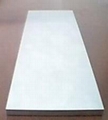
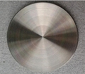
High-purity Nickel (Ni) Target Material for Scientific Research and Experimentation, Magnetron Sputtering PVD Vacuum Coating Target, Vacuum-melted Alloy Target, Purity 99.99%, Customizable Size with Backing Plate Bonding Service
Nickel (Ni), a silvery-white metallic element, boasts unique physical and chemical properties, making it widely applied in the field of target materials. Nickel targets, characterized by their high purity, high density, and relatively high melting point, exhibit outstanding application advantages in numerous high-tech and industrial sectors. Our company specializes in research, development, and production, crafting industry-leading products. We produce single-element targets and electron beam evaporation pellet materials as follows:
SINGLE ELEMENTS: Single-material targets and electron beam evaporation pellets
Aluminum (Al) | Nickel (Ni)
Antimony (Sb) | Niobium (Nb)
Arsenic (As) | Osmium (Os)
Barium (Ba) | Palladium (Pd)
Beryllium (Be) | Platinum (Pt)
Boron (B) | Rhenium (Re)
Cadmium (Cd) | Rhodium (Rh)
Carbon (C) | Rubidium (Rb)
Chromium (Cr) | Ruthenium (Ru)
Cobalt (Co) | Selenium (Se)
Copper (Cu) | Silicon (Si)
Gallium (Ga) | Silver (Ag)
Germanium (Ge) | Tantalum (Ta)
Gold (Au) | Tellurium (Te)
Hafnium (Hf) | Tin (Sn)
Indium (In) | Titanium (Ti)
Iridium (Ir) | Tungsten (W)
Iron (Fe) | Vanadium (V)
Lead (Pb) | Yttrium (Y)
Magnesium (Mg) | Zinc (Zn)
Manganese (Mn) | Zirconium (Zr)
Molybdenum (Mo)
II. Material Characteristics:
Firstly, the high purity of nickel targets stands out as a key highlight. Advanced processes such as electrolytic deposition and sputtering deposition are employed in target preparation to achieve nickel targets with purities up to 99.999% or even higher. During the sputtering coating process, high-purity nickel targets provide a stable and pure stream of nickel atoms, ensuring the formation of high-quality and consistent films on the substrate. This is particularly crucial in semiconductor manufacturing and integrated circuit fabrication, where even minute impurities can affect the performance and stability of the final product. High-purity nickel targets also reduce defects and impurities in the film, enhancing its electrical conductivity, thermal conductivity, and mechanical properties, thereby providing a solid foundation for subsequent processing and applications.
Secondly, the high density of nickel targets is another important physical characteristic. With a density of approximately 8.908g/cm³, nickel targets offer stable sputtering rates and uniform film thickness during the sputtering process. The high density also means that nickel targets can better withstand high-energy ion bombardment during sputtering, reducing target wear and peeling, and thereby extending the target's service life. This characteristic is particularly important for sputtering equipment that requires long-term stable operation, as replacing targets is not only time-consuming and labor-intensive but also affects production efficiency and product quality.
Furthermore, nickel has a relatively high melting point of approximately 1453°C, which enables nickel targets to maintain their physical and chemical stability in high-temperature environments. During the sputtering coating process, the target absorbs a significant amount of energy, which is converted into heat. The excellent thermal conductivity of nickel targets effectively dissipates this heat, preventing the target from overheating and ensuring stable film preparation. Additionally, high-temperature stability means that nickel targets do not undergo unwanted chemical reactions due to high temperatures during sputtering, thereby guaranteeing the purity and performance of the film.
III. Industry Applications:
In the industry, the application advantages of nickel targets are mainly reflected in the following aspects. Firstly, in the semiconductor and integrated circuit manufacturing sectors, nickel targets are widely used to produce high-quality conductive layers due to their high purity and good electrical conductivity. These conductive layers play a crucial role in connecting and transmitting signals within chips, and their quality and stability directly impact the performance and reliability of the chips.
Secondly, in the magnetic material preparation field, nickel targets are extensively applied in the manufacture of products such as hard disk drives and magnetic storage devices due to their unique ferromagnetic properties. The high magnetism and stability of nickel targets enable these products to have higher storage densities and read/write speeds, thereby enhancing data transmission efficiency and security.
Moreover, nickel targets are widely used in the manufacture of thin-film solar cells, optoelectronic memory devices, flat-panel displays, and other electronic products. In these fields, the high corrosion resistance of nickel targets and the high-precision sputtering film formation technology contribute to the better durability and stability of these products, thereby extending their service life and enhancing user experience.
In summary, nickel targets, with their high purity, high density, and relatively high melting point, exhibit outstanding application advantages in multiple fields such as semiconductor manufacturing, magnetic material preparation, and electronic product manufacturing. As technology advances and market demands change, the preparation technology and application fields of nickel targets will continue to expand and improve, providing superior material support for the development and production of more high-tech products.
| Payment Terms: | TT |
|---|---|
Member Information
| Suzhou Zhongzhina Semiconductor Technology Co., Ltd. | |
|---|---|
| Country/Region: | Jiang Su - China |
| Business Nature: | Manufacturer |
| Phone: | 95613164 |
| Contact: | spring (Jiangsu Province) |
| Last Online: | 17 Feb, 2025 |
Related Products of this Company
-
sputtering strontium barium titanate
-
PVD Magnetron Sputtering Coating Target
-
Copper Indium Selenide Target,
-
Molybdenum-Niobium Target, Niobium Oxide
-
The translations for the given terms are
-
The translations for the given terms are
-
Zinc aluminum oxide target, zinc oxide
-
The translations for the given terms are
-
Indium Tin Oxide Target Magnetron
-
Iridium target, platinum target,


